Wednesday, October 31, 2012

Project Testing


After all the wiring and fitting completed, continuity test , provide supply , trib test done.. now it is the time to go to the final element, project test. Project will given up supply of a 240V and a load of 100Watts of bulb which is 6 bulbs overall total 600 watts. Once switch is turn on, all the bulbs is lights up.

Measuring total Amps in the circuit using clamp meter.
 

The output of the socket is 235V  as same as the input supply


Display read the meter well displaying the consumption power, value of kWh that had been used and the total value of the usage in Ringgit Malaysia

Tuesday, October 23, 2012

Hardware Development : Fitting and Wiring


After all the electrical stuff i had, i begin with  the box to place the circuit for Kwh meter.

then i place the distribution box next to the KwH box


 Wiring the connection for Main switch, Earth leakage circuit breaker, and Main circuit breaker. After done the wiring, do the continuity test again to check all the connection is good.


Drilling hole for fitting the bulb, switch and socket.


Fitting the bulb wire

Finalize the Hardware development .

Saturday, October 20, 2012

Hardware Developement : contuinity test


To check the connectivity, i perform a continuity test, continuity test is  checking of an electric circuit to see if current flows (that it is in fact a complete circuit). A continuity test is performed by placing a small voltage (wired in series) across the chosen path. If electron flow is inhibited by broken conductors, damaged components, or excessive resistance, the circuit is "open".
Devices that can be used to perform continuity tests include multimeters which measure current and specialized continuity testers which are cheaper, more basic devices, generally with a simple light bulb that lights up when current flows.
An important application is the continuity test of a bundle of wires so as to find the two ends belonging to a particular one of these wires; there will be a negligible resistance between the "right" ends, and only between the "right" ends.


When the continuity test done, i give them load to prove the continuity test  achieved. 240v supply connection applied (life,neutral and ground). i use test pen to complete the task. once i touch at the end poit of test pen the light is on which means the connection is good at no leakage voltage.

Monday, October 15, 2012

Hardware Development : Electrical Appliance


Electrical Appliances
  1. Main switch
  2. Earth Leakage Current Breaker (ELCB)
  3. Main Circuit Breaker (MCB)10A,16A
  4. Electrical Deck Box
  5. Bulb Holder
  6. Bulb (100watts)
  7. 2.5mm wiring cable
  8. 1.5mm wiring cable
  9. Switch box
  10. socket box
  11. wooden layout 

Monday, October 8, 2012

Software Development : Program the PIC


For software development i used MikroC, MikroElektronika C compiler for microchip PIC microcontrollers version : 8.0.0.0.

 
 I use basic C language for my project programming for PIC Microcontroller. after completed all of the program without any error( save file as .c), then compile all and proceed to burn HEX file to my PIC16F877A


  1.  Import the HEX file
  2. Reading the device and memory.


  1.  verifying the device and memory
  2. program was successful write into microcontroller.


The PIC Burner that i used to burn HEX file.

Saturday, September 29, 2012

Circuit Design Part 7 : Soldering component


Soldering is defined as "the joining of metals by a fusion of alloys which have relatively low melting points". In other words, using a metal that has a low melting point to adhere the surfaces to be soldered together. Consider that soldering is more like gluing with molten metal, unlike welding where the base metals are actually melted and combined. Soldering is also a must have skill for all sorts of electrical and electronics work. It is also a skill that must be taught correctly and developed with practice.   


Soldering components onto a PCB involves preparing the surface, placing the components, and then soldering the joint.

Step 1: Surface Preparation:
 A clean surface is very important if you want a strong, low resistance solder joint. All surfaces to be soldered should be cleaned well.

Step 2: Component Placement:
After the component and board have been cleaned,its ready to place the components onto the board.

Step 3: Apply Heat:
Apply a very small amount of solder to the tip of the iron. This helps conduct the heat to the component and board, but it is not the solder that will make up the joint.

Step 4: Apply Solder To The Joint :
Once the component lead and solder pad has heated up, you are ready to apply solder. Touch the tip of the strand of solder to the component lead and solder pad.

Step 5: Inspect The Joint and Cleanup:
Once the surface of the pad is completely coated,the joint is made and should inspect it.

Tuesday, September 18, 2012

Circuit Design Part 6 : Drilling PCB board


Remove the coloured part that covered the cooper with Silicon Carbide Abrasive paper. Once it done proceed with drilling procedure.


Drilling with 0.8mm drill bits can be a bit tricky as it's easy to break the drill bits. Always hold the drill straight and do not bend it when the hole has started. Putting a soft block of wood under the PCB provides a good base to drill into.

1. Dry off the board and clean away the blue etch resist with brush. 
  2. Using a 0.8mm PCB drill bit drill out all of the component holes  
3. Some 1mm holes may need to be made for connectors, 3mm for corner fixings
4. Finally use a PCB rubber to clean the copper ready for soldering

So now PCB's finished and you can start soldering the components in. You should do this soon after you have cleaned the PCB (within 1 hour) as the copper soon oxidises and becomes hard to solder onto.

Saturday, September 15, 2012

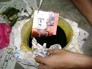
Circuit Design Part 5 : Etching process

 Ferric Chloride

The basic principle of etching any metal is to apply a substance to the surface of the metal which will rOne of the most discouraging things about making a hardware project (apart from obtaining all of the components) is building the printed circuit board - PCB.  It is sometimes possible to use strip board or some other pre-fabricated board but more often than not the circuit complexity and performance requires a proper PCB to be made.  The good news is that due to improvements in printing and processing technologies it is now relatively easy to make inexpensive high quality PCB's at home.Making PCB's requires the use of Ferric Chloride (FeCI3) which is corrosive so avoid skin and eye contactesist the bite of the etching solution. This substance is called resist. Once the resist is applied, all you have to do is submerge the piece in the etching solution and wait for it to etch.


Etching Steps
  1. Dilute the concentrated Ferric Chloride fluid with water and pour into the
        container.
  2. Place a sheet of news paper on a flat surface and put the trays on it's.
  3. Put the PCB copper side up into Ferric Chloride.
  4. Hold the PCB board with metal holder.
  5. Gently rock the top tray to keep the etch fluid moving avoiding spillage.
  6. After about 15mins all of the unwanted Copper should have disappeared.
  7. Remove the board and drop it into a bucket of cold water to clean off. 
 The final touch.

Tuesday, September 4, 2012

Circuit Design Part 4 : PCB layout to PCB board

1. PCB layout design is printed out using laser jet to the sticker sheet.

 2. PCB layout to PCB board
3. PCB board is placed at printed surface before heat procedure.

4.  Using an iron to get the heat for easier printed layout placed to PCB board.

 5. The final touch

Wednesday, August 29, 2012

Circuit Design Part 3: Assembly variants/component


Assembly Variants.
  1. Quick connectors
  2. Rectifier
  3. Capacitors
  4. Diode
  5. Lcd Display 16*2
  6. Fuse
  7. Pic 16F877A Microcontroller
  8. Voltage Regulator
  9. Inductor
  10. LED
  11. Resistor
  12. Potentiometer
  13. Switch
  14. Transformer
  15. Current Tranducer

Monday, August 13, 2012

circuit design Part 3 : LTS 25-np


Current Tranducers for the electronics measurement of current : DC, AC, Pulsed, mixed with galvanic isolation between the primary circuit (high power) and secondary circuit (electronic circuit)

Friday, August 10, 2012

circuit design Part 2 : PCB layout

circuit design part 2 is about the conversion of schematics design to board design.

Schematics design to Board design.

when the selection of the components link connection is completed, the next step is converting to PCB layouts.


this is the final design of PCB layouts before it print out to PCB board.


Wednesday, August 1, 2012

circuit design part 1


 i start my second part of my final year project by designing circuit schematic. i used EAGLE ( Easy Applicable Graphics Layout Editors as a schematic designer. this software is developed by http://www.cadsoftusa.com. The component libraries supplied with EAGLE have been compiled with great care as an additional service to me. However, the large number of available components and suppliers of these components means that the occasional discrepancy is unavoidable.  

 after the designing is completed. i have to convert it to the PCB layout. this step will show the link or connection between component before do the etching process.

Saturday, April 14, 2012

Analouge Meter


For some reason, i have to change the from digital meter to analogue meter due the high cost of digital meter. It is about RM 1+++. Actually there is no different with digital meter as long as i can get the same accurate output at the display.

General Description
  • The Single-phase Kilowatt-hour Meter Type DD28 is an instrument of induction type, used for measuring the singlephase.A.C. energy of rated frequency 50Hz.The instrument is novel design, attractive appearance, compact and sturdy construction. The instrument features high.accuracy, over wide load range and a long service life. All the components of this meter are of selected material and the metal ones electroplated or finished with baking enamel. The casing and terminal block with gasket are properly treated against mould, moisture and dust.
Technical Characteristics
a. Sensitivity
When the meter is running with 0.5% rated current at rated voltage and frequency and unity power factor, the rotor willrotate ceaselessly.

b. Running with No Loading
With no current in the current circuit, the rotor will not make a complete revolution at any voltage between 80% and110% of rated voltage.

c. Power Consumption
With no current in the current circuit, the power consumption of the voltage circuit is within 1.5W at rated voltage and frequency.With rated current circuit, the power consumption of the current circuit is within 2VA at rated frequency.

d. Insulation Test
With the specified ambient temperature and relative humidity below 85%, the insulation between the casing and all the circuits can withstand a test of 2kV, 50Hz for 1 min.

Estimated Project Cost

Table shown the estimated cost for completing the project. Any additional cost may accure during the progress to finalize the device.

Overall total is RM 574.00

Expected result

  1. When the device complete in terms of the system design, we can get an accurate amount of usage in a display meter.
  2. From the usage amount, the device is set to the same rate per block as TNB rates of electricity.
  3. The value of the electricity usage will display in Ringgit Malaysia.
  4. This device can be implement in a future development of nation electricity field. Reliability estimation was found to be the one of the best method to know the usage of electricity, a monitor that gives a real time feedback on how we consuming in our usage.

Home

Office

Factory